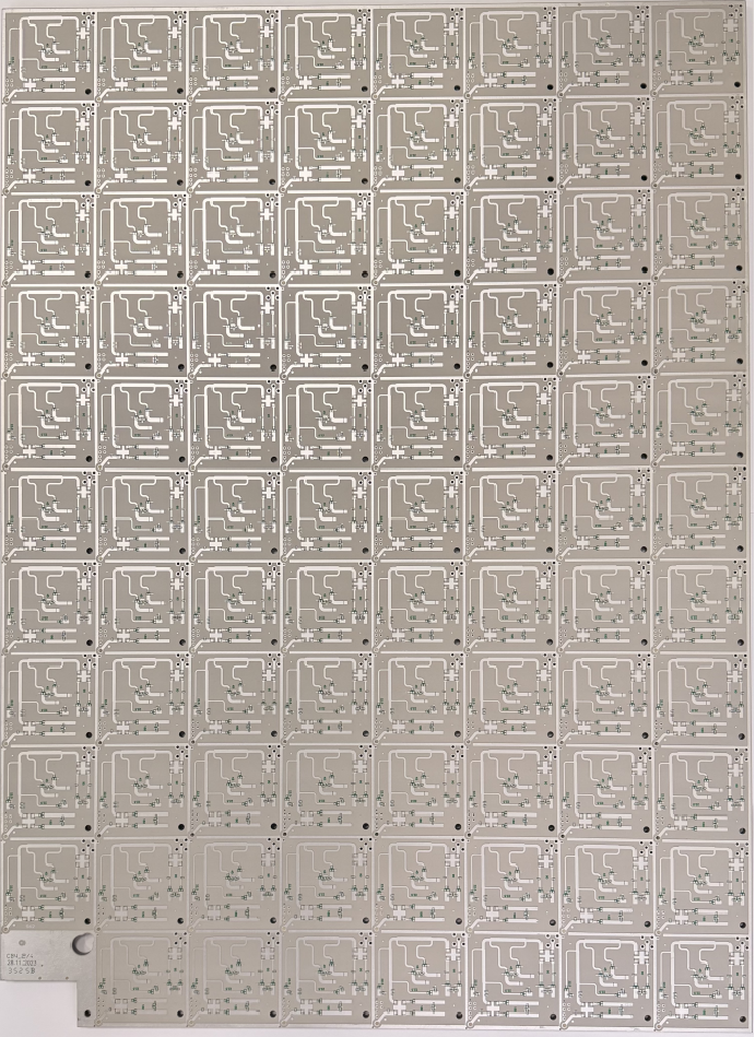
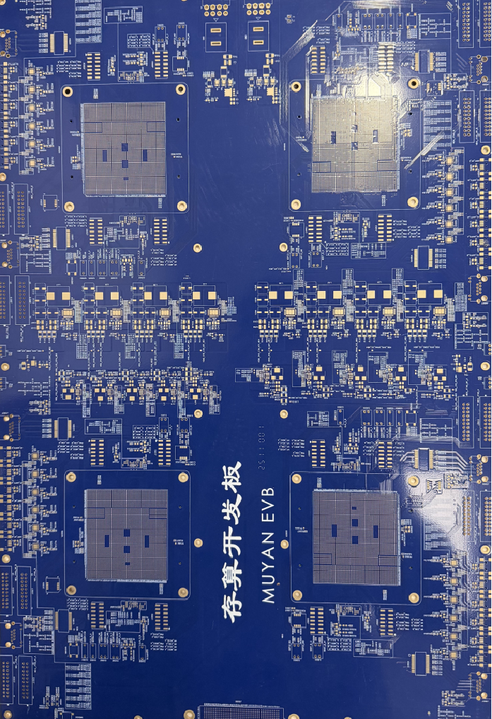
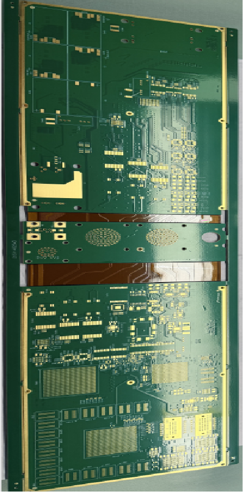
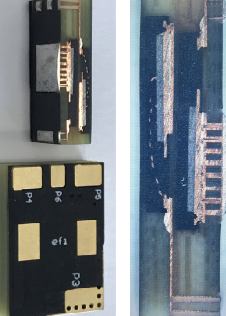
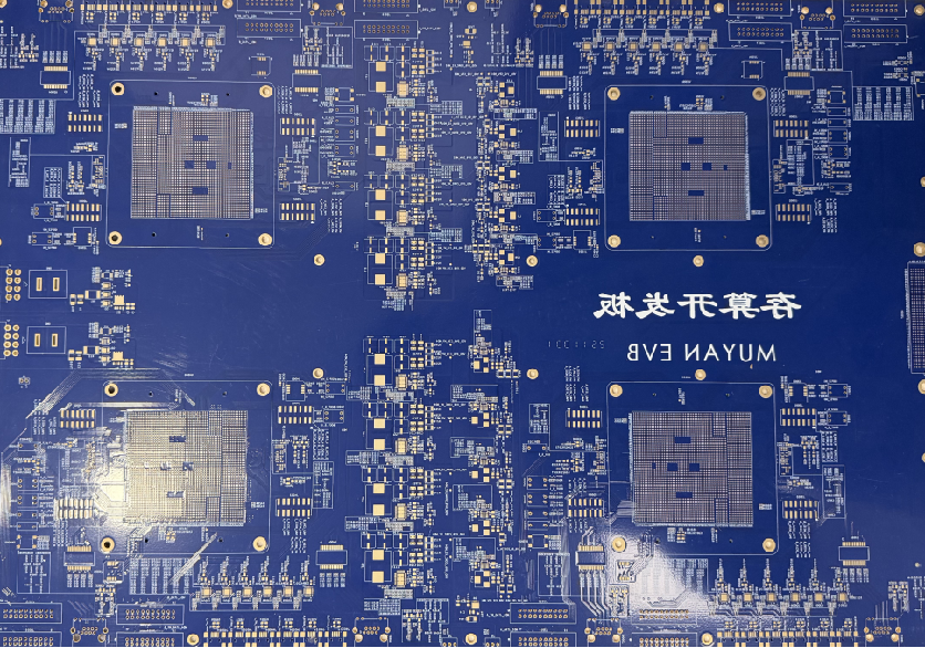
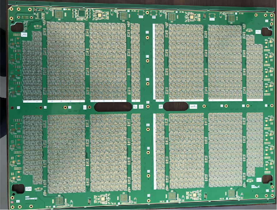
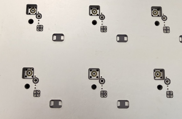
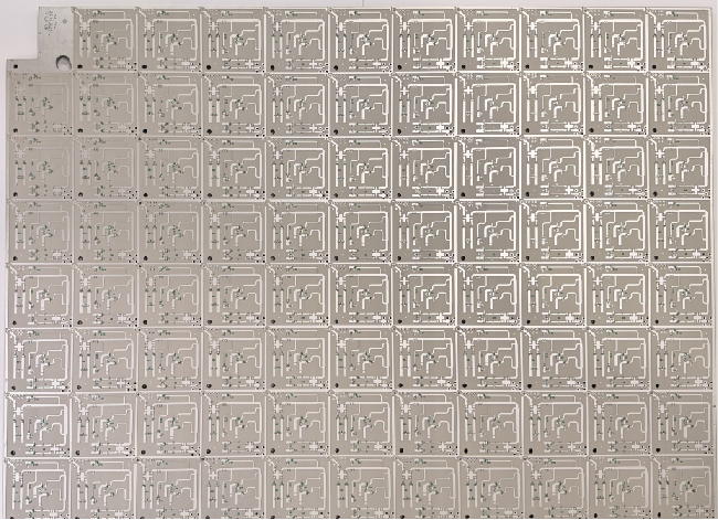
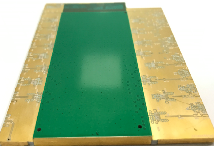
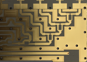
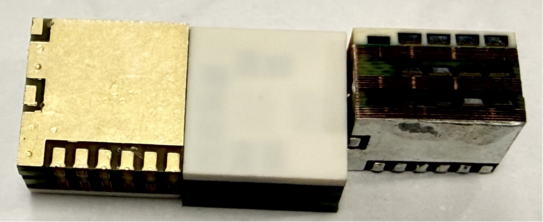
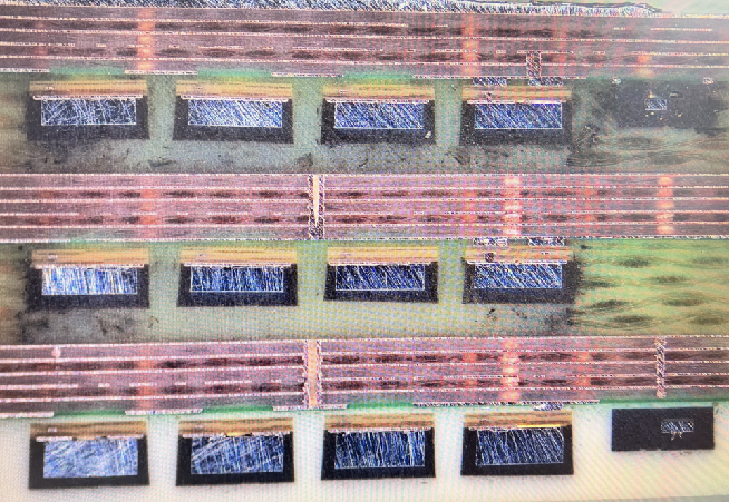
Our products focus on high multi-layer boards, high-frequency microwave PCBs, high-speed signal transmission PCBs, blind & buried via boards, high thermal conductivity metal substrates, flexible and rigid-flex PCBs.
| High-Frequency Microwave PCB | High-Speed Multi-Layer PCB | Flexible PCB | Special Structure Products |
|---|---|---|---|
|
• Various step slot & multi-step slot processes • Pure gold plating process • High-position precision graphic processing • High line width precision control • Laser contour process • Thick & thin gold combination plating • Metal edge wrapping process • Glue overflow control • Various surface finishing technologies • Expansion & shrinkage control system • Various surface finishing technologies |
• High-precision impedance technology • High-precision patterning technology • High-precision alignment technology • High aspect ratio drilling (drilling, PTH, electroplating) |
• Lamination process • Hollow board process • Slotting process • Oversize process |
• Embedded component lamination technology • Copper paste plugging technology • Copper block embedding technology • Copper paste sintering technology |
Advanced manufacturing processes meeting full-range high-precision PCB production from prototype to mass production
| Category | Prototype | Low Volume / Mass Production |
|---|---|---|
| Layers | 1-40 layers | 1-32 layers |
| Materials | High-frequency / High-speed / Metal substrate / FR4 (Tg140, 150, 170, 250) / Halogen-free | High-frequency / High-speed / Metal substrate / FR4 (Tg140, 150, 170, 250) / Halogen-free |
| Max Panel Size | Single: 1500×5500mm Double: 620×1800mm Multi-layer: 620×1200mm | Single: 1500×5500mm Double: 620×1800mm Multi-layer: 620×1200mm |
| Board Thickness | 0.025mm-10.0mm | 0.025mm-10.0mm |
| Max Finished Copper | Inner 6oz, Outer 14oz | Inner 6oz, Outer 14oz |
| Min Drill Diameter | 0.1mm | 0.1mm |
| Aspect Ratio | 25:1 | 20:1 |
| Min Line Width / Spacing | 3.0mil / 2.0mil | 3.0mil / 3.0mil |
| Min Solder Mask Bridge | 3mil | 3mil |
| POFV Via Diameter | 0.20mm-1.2mm | 0.20mm-1.2mm |
| Impedance Control | ±5% | ±10% |
| Solder Mask Color | Green / White / Black / Red / Yellow / Blue / Purple / Matt Green / Matt Black... | Green / White / Black / Red / Yellow / Blue / Purple / Matt Green / Matt Black... |
| Surface Finish | ENIG / ENEPIG / Electroplated Pure Gold / Electroplated NiAu / Immersion Silver / Electroplated Silver / Immersion Tin / Electroplated Tin / EGold+IGold / IGold+OSP / Leaded HASL / Lead-free HASL / OSP | ENIG / ENEPIG / Electroplated Pure Gold / Electroplated NiAu / Immersion Silver / Electroplated Silver / Immersion Tin / Electroplated Tin / EGold+IGold / IGold+OSP / Leaded HASL / Lead-free HASL / OSP |
Weapon systems, communication systems
Aerospace ceramic substrates, avionics, satellite communications
Base station antennas, RF microwave, power amplifier modules
24/77GHz automotive radar, ADAS systems
Imaging equipment, in-vitro diagnostics, monitoring instruments
Navigation systems, shipboard communications, marine radar